
esting After PCB Design and Assembly
When a PCB goes through a series of inspection and testing procedures, it makes sure that the design has been implemented properly. This process helps to minimize errors that could cost time, money and quality issues in the production of a final product.
Once the layers of the pcb design and assembly are placed, the assembly process begins. The bare board is tested with various methods, including optical inspection and functional testing. This testing ensures that all components are placed correctly and that the board works as expected. The process also verifies that the fabrication-assembly process has been executed correctly.
For example, optical inspection is a machine-based process that scans the layers of the board to ensure they are free of any defects in both top and bottom surfaces. It checks the physical parameters of each layer to find if there are any scratches, incorrect mask application and soldering or joint problems. A computer then compares the digital image of the layer to the original Gerber file that the manufacturer received. If the images do not match, the layer will fail to pass inspection and must be manually reworked before continuing.
Another type of test is called in-circuit test (ICT), which verifies the positioning and fitment of each electronic component on the pcb. This test includes checking for short circuits, open ends, resistance and capacitance. This is typically performed using a flying probe system, which uses an array of drivers and sensors that move freely on the surface of the board. This method is also a reliable way to check for mechanical components mounted after the bare board assembly, such as connectors and other metal parts.
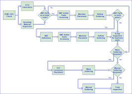
Types of Testing After PCB Design and Assembly
Other types of tests that are commonly performed on a pcb include a X-ray test, which shows the internal structure of the pcb to identify defects. Another test is a temperature rise test, which simulates environmental conditions such as extreme temperatures and humidity, to see how the pcb will respond in these conditions. This is an important test for critical pcbs, such as those used in medical devices or military equipment.
Choosing the right components for a pcb is crucial to its function and longevity. It is best to choose standard or common components that can be easily sourced from multiple manufacturers. This will increase the quality of the finished product, reduce inventory costs and speed up the production process. However, custom or unique parts are sometimes required in order to meet specific design requirements. It is best to keep these in mind during the design phase and avoid selecting components whose shelf life is approaching an end.
Functionality tests are the most common type of tests that a pcb undergoes. These are designed to verify the pcb’s functionality and can be customized for each client’s unique requirements. Using these tests early in the design process can help to identify possible problems and allow for timely and effective corrections to be made before the production process starts. This can also reduce rework time, which is essential to maintaining a fast, high-quality manufacturing process.


